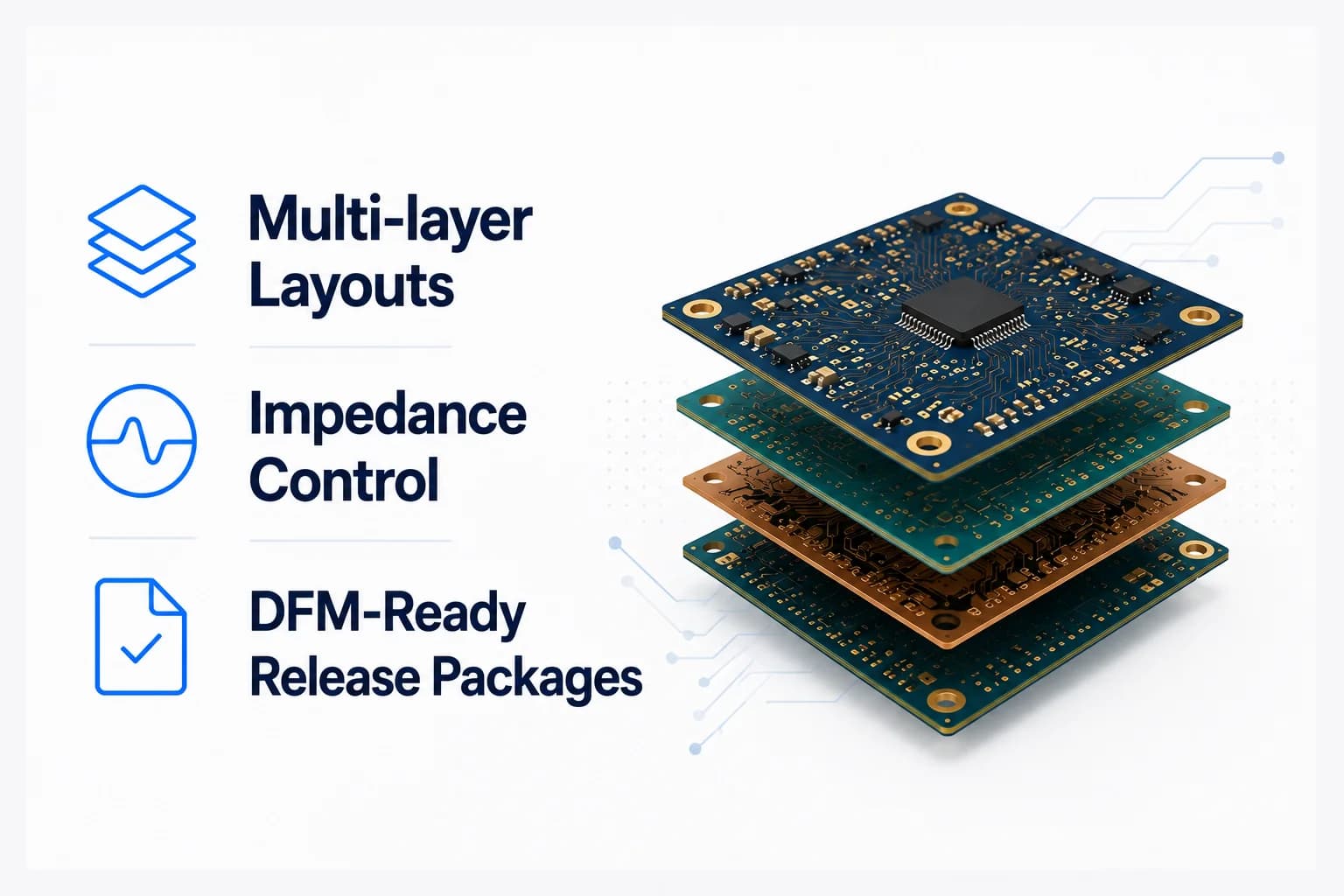
PCB Design
Multi-layer layouts, impedance control, and DFM-ready release packages.
Engineering · PCB · IoT Hardware
SDI designs production-ready printed circuit boards and connected hardware platforms — from architecture and schematic capture through layout, bring-up, and factory release.
Whether you need a sensor node, gateway, edge controller, or full IoT product stack, our engineering team unites electronics, embedded software, and manufacturing discipline under one program.
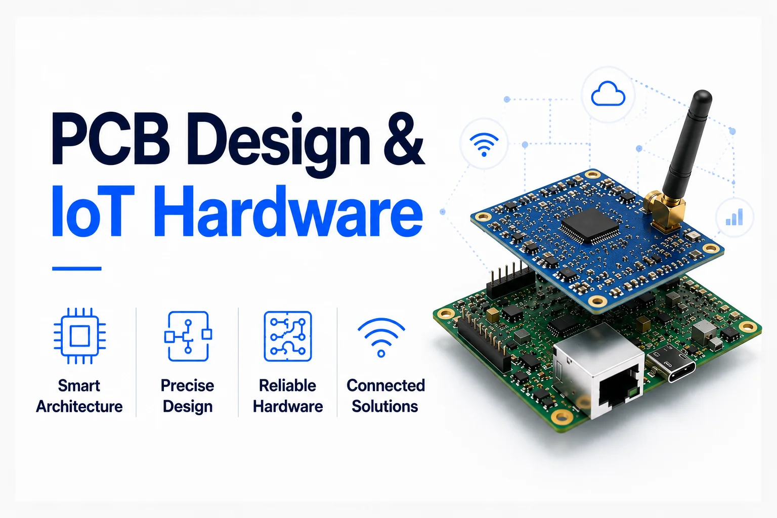
Real-world IoT products fail when schematic choices, RF layout, power architecture, and firmware assumptions are made in isolation. SDI coordinates every layer — electrical, mechanical, thermal, and software — before the first spin.
Our multidisciplinary approach de-risks BOM cost, certification paths, and factory testability early, so your platform scales from pilot builds to volume without redesign cycles.
Cross-domain hardware programs spanning board design, embedded systems, and connected product platforms.
Multi-layer layouts, impedance control, and DFM-ready release packages.
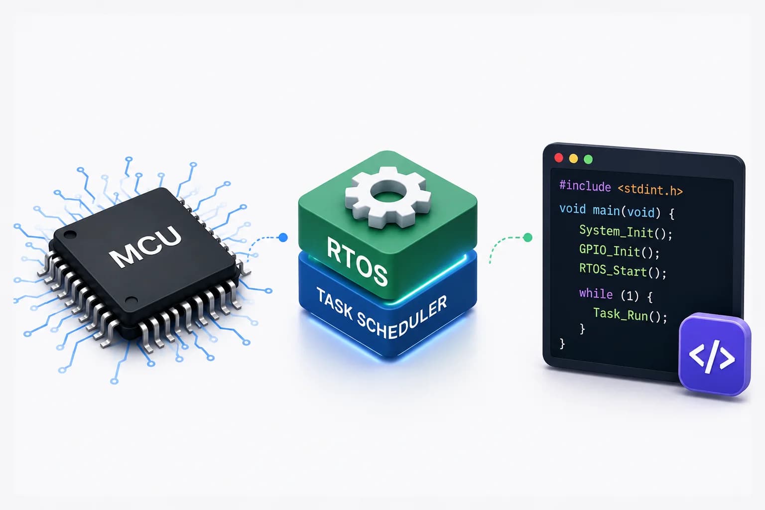
MCU selection, RTOS integration, and production firmware architecture.

Connected products with provisioning, OTA, and secure device identity.
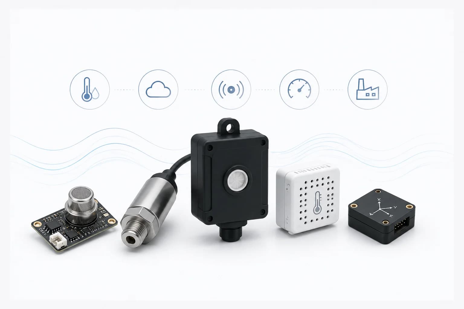
Environmental, motion, and industrial sensing with calibrated signal chains.
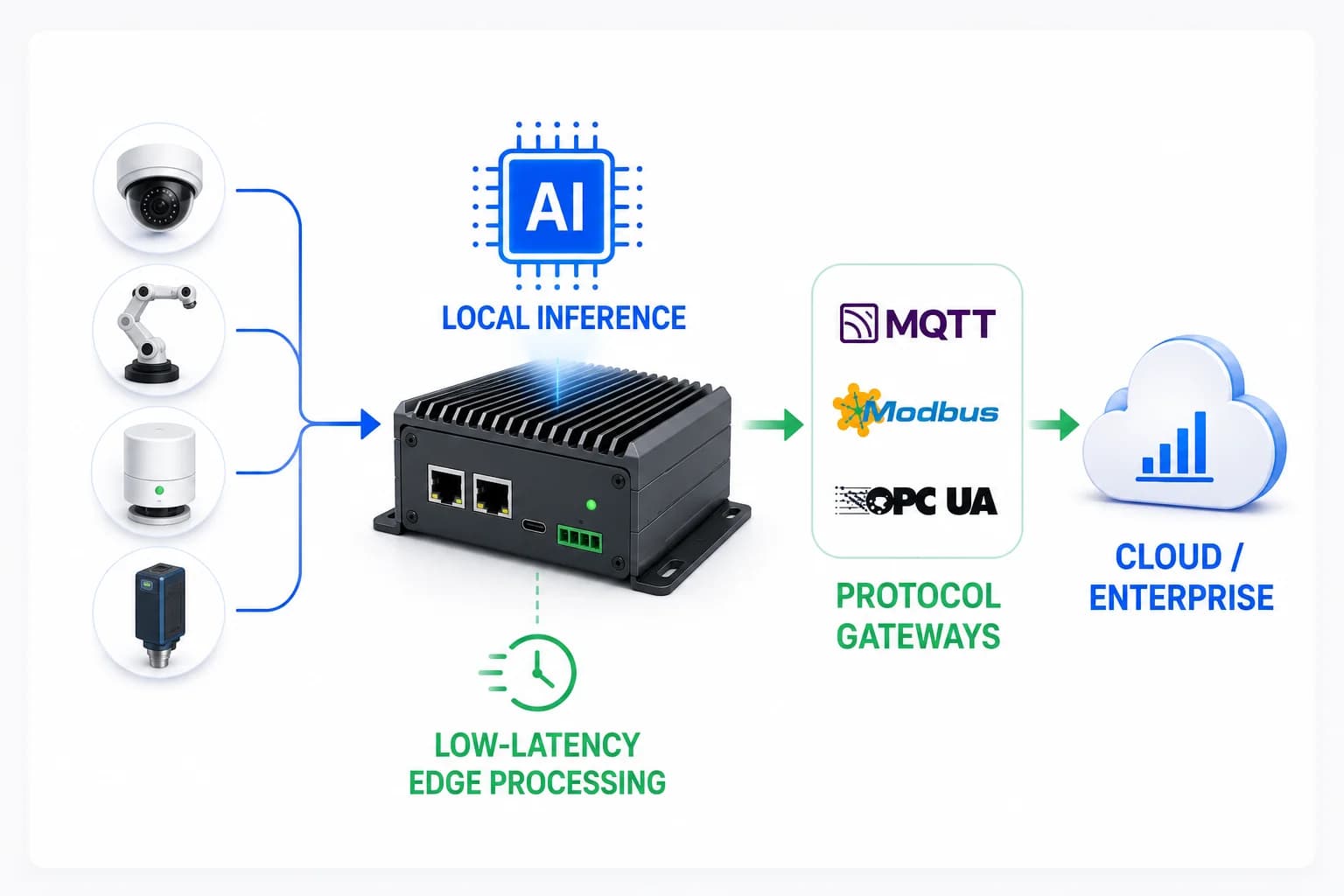
Local inference, protocol gateways, and low-latency edge processing.

Functional engineering builds for validation before production tooling.
Core differentiators from first architecture decisions through factory preparation.
Block diagrams, power budgets, and interface definitions aligned to product requirements.
Reviewed schematics with BOM optimization and component lifecycle analysis.
Controlled impedance, RF keep-outs, thermal paths, and assembly-friendly placement.
Bootloader, drivers, and communication stacks validated on first article hardware.
Environmental, EMC prep, and functional test fixtures for repeatable QA.
Gerber releases, assembly drawings, test procedures, and vendor handoff packages.
Protocols, processors, and sensor families we routinely design into connected hardware platforms.
Full lifecycle support mapping hardware through software, cloud, and manufacturing.
Schematic, layout, and production release.
Embedded drivers, RTOS, and device logic.
Provisioning, dashboards, and user-facing control.
Telemetry pipelines, device management, and APIs.
Edge inference and cloud model integration.
DFM, factory selection, and pilot-to-volume ramp.

Senior hardware architects in California lead design reviews and program direction.
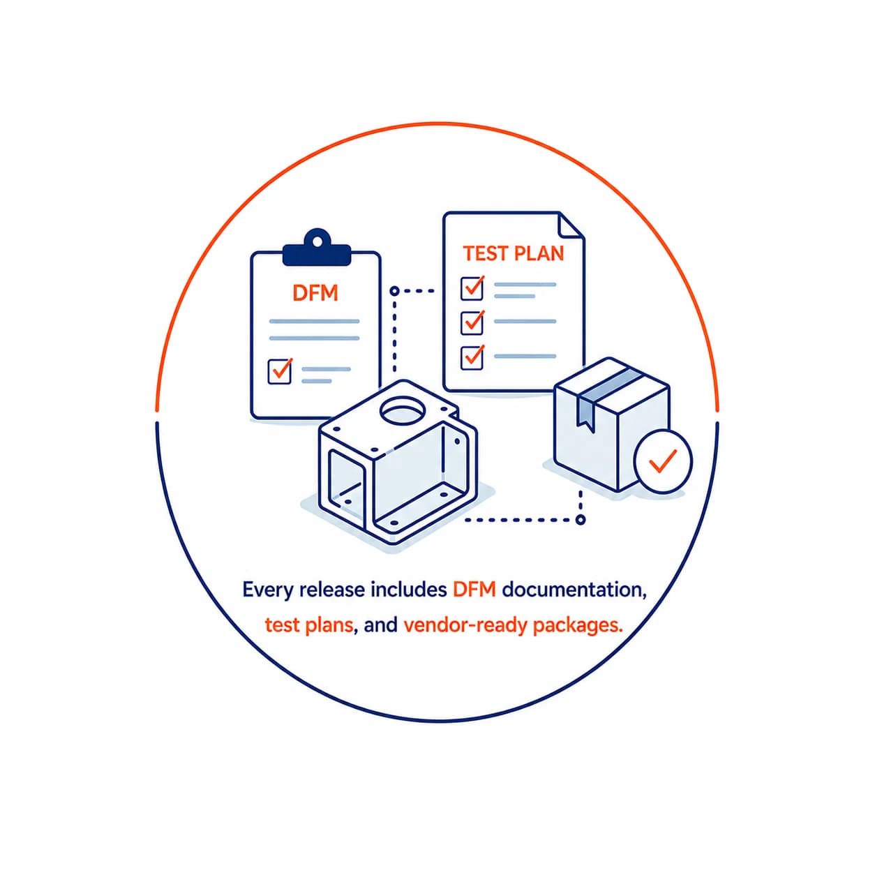
Every release includes DFM documentation, test plans, and vendor-ready packages.

Factory partners across Asia and domestic options for scalable builds.
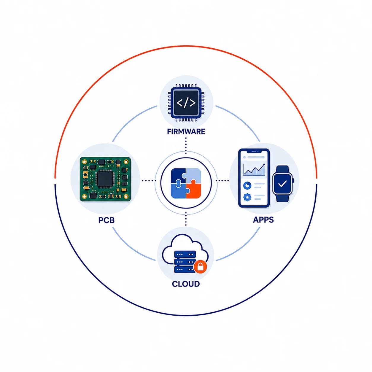
PCB, firmware, apps, and cloud coordinated as one integrated program.
Share your architecture, reference design, or product requirements. Our team will scope PCB, firmware, and IoT integration as one program.
Request Free EstimateCommon questions about PCB design, IoT hardware, timelines, and production handoff.
Architecture, schematic capture, multi-layer layout, SI/PI review, prototype coordination, and factory-ready Gerber releases.
Yes. We integrate Wi-Fi, Bluetooth, LoRa, cellular, Thread, Matter, and other protocols with antenna and certification planning.
We audit and improve existing designs for cost, reliability, manufacturability, and firmware compatibility.
Yes. Embedded bring-up, drivers, RTOS, and communication stacks are part of our hardware programs.
ESP32, nRF52, STM32, NXP i.MX, Raspberry Pi compute modules, TI, Microchip, and Qualcomm platforms among others.
Signal conditioning, calibration, fusion algorithms, and mechanical placement coordinated with industrial design.
We implement edge inference pipelines on capable MCUs and companion processors with cloud fallback.
Gerbers, assembly drawings, BOM, test procedures, firmware images, and vendor communication support.
First-spin hardware often ships in 8–14 weeks depending on complexity, RF requirements, and certification scope.
Submit your requirements through our contact form with target volume, timeline, and any reference designs.